Components / BJTs

BJTs: NPN, PNP and Basic Operation

Learn base drive, collector current, saturation and package pinout checks.

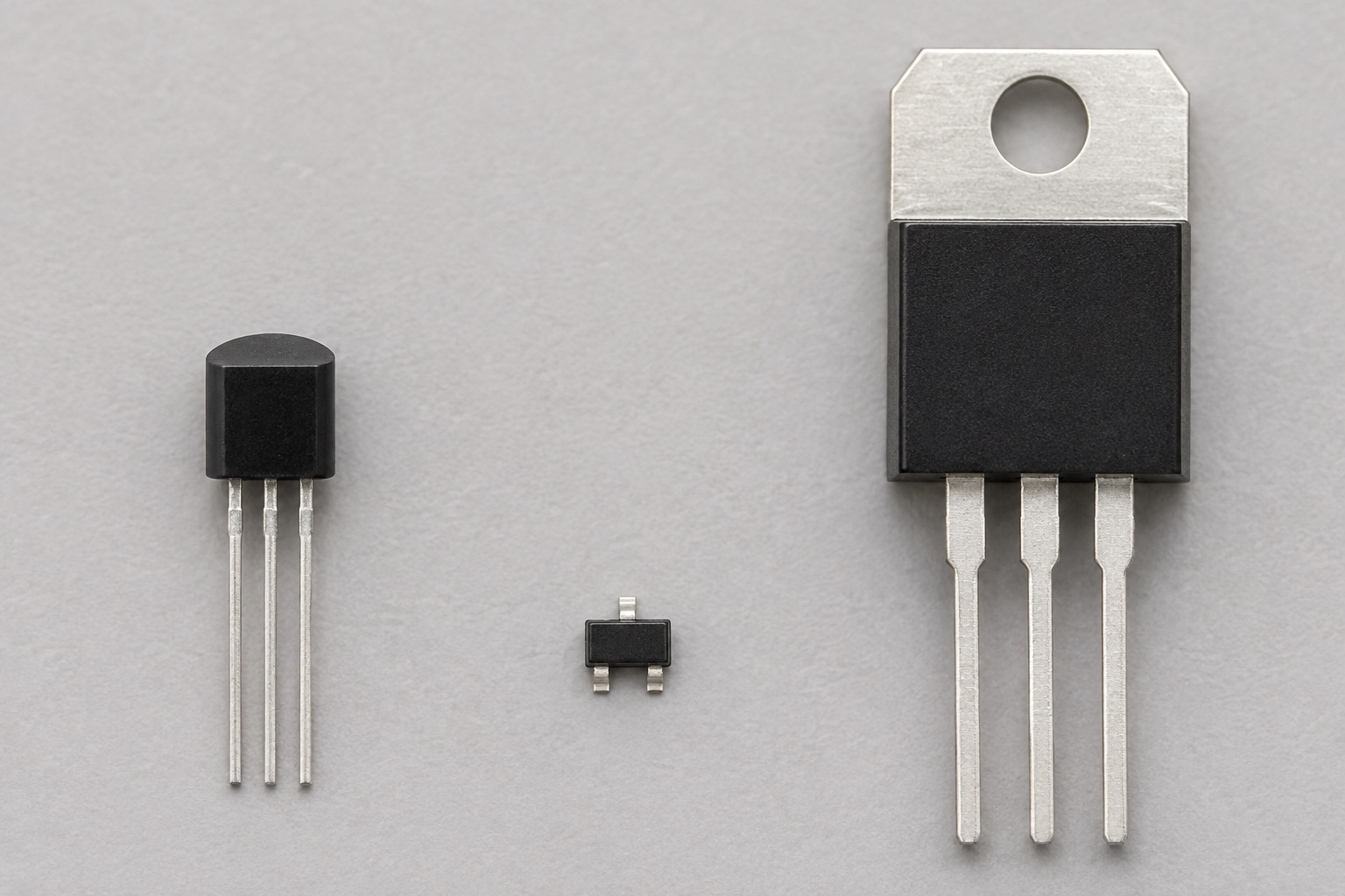
Illustrated bipolar transistor packages: small TO-92 at left, tiny SOT-23 in the centre and larger TO-220 at right
Appearance illustration of 3 common physical forms. Generated for teaching, not a photograph of the models below; size and markings are not exact. See the in-site model notes for verified details.

Recognise and choose

What forms will you encounter?

01Small three-lead package, left

TO-92 through-hole transistor

How to recognise it
Black half-round plastic body with three leads.
Use it when
Breadboard experiments and low-power switching or amplification.
Check before choosing
NPN versus PNP, lead order, collector current and dissipation.

Model notes on this siteonsemi 2N3904 (NPN) →

02Tiny three-terminal package, centre

SOT-23 surface-mount transistor

How to recognise it
Small flat black body with three gull-wing contacts.
Use it when
The same basic transistor functions on compact assembled PCBs.
Check before choosing
Pin map, gain group, saturation data and board thermal limits.

Model notes on this siteNexperia BC817 (NPN) →

03Large tabbed package, right

TO-220 power transistor

How to recognise it
Three leads and a metal mounting tab with a screw hole. A TO-220 MOSFET can have the same exterior.
Use it when
Higher-current loads with a thermal design that may include a heatsink.
Check before choosing
Read the part marking and model-specific Base–Collector–Emitter pin diagram; also check the tab connection, safe operating area, base drive and heat.

Model notes on this siteSTMicroelectronics TIP41C (NPN) →

At a glance

A bipolar junction transistor uses base current to control collector current. It can amplify a signal or switch a load when driven appropriately.

This guide explains a component family. Check the exact part number and manufacturer datasheet before building.

Key specifications

VCEO
Maximum collector-emitter voltage with base open
Collector current (Ic)
Current limit under stated thermal conditions
DC gain (hFE)
Amplifier-region gain at specified Ic and VCE
VCE(sat)
Collector-emitter drop with specified collector and base currents

Circuit Lab

Put this component into a circuit

How much base drive is needed for a saturated BJT switch?

Change
Supply, load current, base resistor and transistor VCE(sat) model
Observe
Base current, forced gain and transistor loss

Explore the linked experiments using their stated model assumptions. Device-specific limits still come from the linked datasheets.

How it works

For an NPN low-side switch, the load connects between supply and collector, the emitter goes to ground, and a resistor limits base current. A PNP counterpart often switches the high side with reversed polarities. Amplifier-region hFE does not guarantee saturation.

Types and construction

Small-signal and power BJTs differ in current, voltage, gain and heat dissipation. NPN and PNP polarities are not interchangeable in the same circuit; even parts with similar names may have different lead orders.

Worked example

For a 5 V logic output, a 1 kΩ base resistor and an assumed 0.7 V base-emitter drop give about 4.3 mA base current. At a 40 mA load this is a forced ratio near 9.3. Confirm the controller can source that current and check the transistor’s VCE(sat) data at comparable conditions.

Reading a datasheet

Read the exact package pin diagram, VCEO, Ic, power dissipation and derating, hFE test conditions, VCE(sat) at stated Ic/IB and safe operating area if supplied.

Common mistakes

  • Using the headline hFE number to size a saturated switch.
  • Omitting the base resistor.
  • Assuming all three-lead transistors share the same pin order.

Explore further

Source and review

Reviewed 18 November 2026 against Nexperia, BC817 series datasheet. Examples are simplified educational models; ratings and pinouts depend on the exact device.