Distinguish gate threshold from full enhancement and check switching losses.
How it works
An N-channel enhancement MOSFET can act as a low-side switch. Its gate draws little steady DC current but must be charged and discharged during switching. The body diode conducts in one direction even when the channel is off.
Types and construction
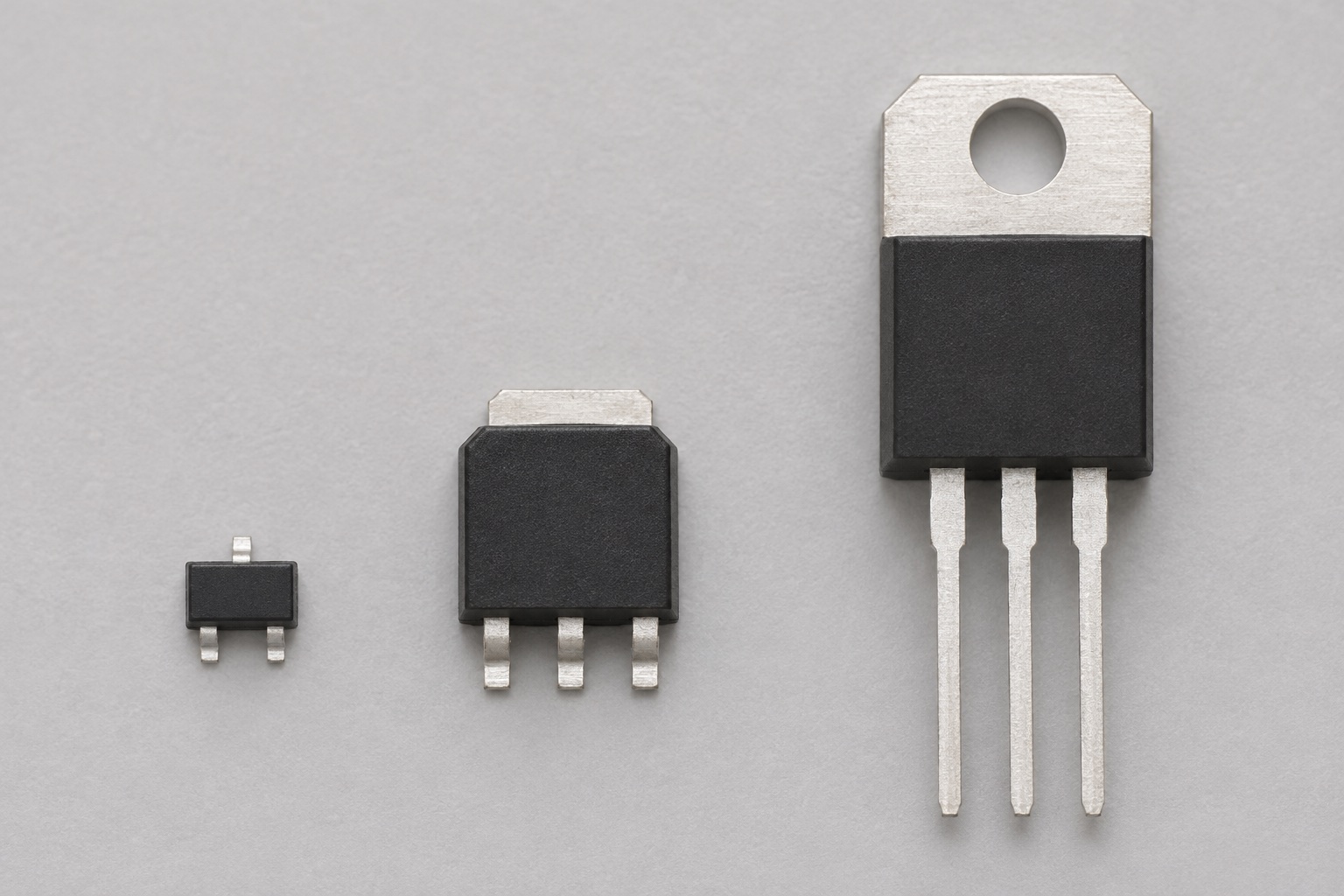
N-channel and P-channel devices use different gate polarities. “Logic level” is a useful label only when RDS(on) is specified at the actual available gate voltage. Power packages and PCB copper strongly affect thermal performance.
Worked example
If a particular MOSFET is specified at RDS(on) = 0.10 Ω for VGS = 4.5 V, then 0.5 A DC produces an idealized 25 mW channel conduction loss (I²R). Recheck RDS(on) at hot temperature, switching loss and package thermal limits before using the result.
Reading a datasheet
Compare VDS margin, maximum VGS, RDS(on) at the available gate drive, total gate charge, body-diode data, safe operating area and thermal resistance. VGS(th) is measured at a small specified drain current and is not a full-on guarantee.
Common mistakes
- Choosing a MOSFET from VGS(th) alone.
- Exceeding the gate-to-source maximum while trying to lower on-resistance.
- Ignoring gate charge, body-diode direction or heat at the real switching frequency.
Explore further
Source and review
Reviewed 18 November 2026 against Texas Instruments, Avoid Common Mistakes When Selecting and Designing With Power MOSFETs. Examples are simplified educational models; ratings and pinouts depend on the exact device.